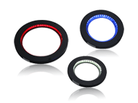
High brightness LEDs are evenly arranged to bring maximun brightness; the light level is illuminated; the object can be highlighted in the working distance of 5-10mm.
Features:*Diverse and customized angle *Simple installation and compact design *High brightness to bring maxium brightness *Optional diffusers to meet the different needs | Applications:》Inspection of IC chips' appearance and character 》Inspection of PCB substrate 》Inspection of product packaging defect 》Inspection of product label 》Microscope illumination 》Inspection of general appearance defect | Application Fields:1.Scratches on the metal surface 2.Character on IC surface 3.The outstanding of the contour |
·KMN-RN0KMN - RN ## ##- R/G/B/W/IR/UV  |
|